The OCP8111B integrates PWM step-less dimming flash driver technology, driving technological innovation in flash fill light modules


As the integration and proliferation of smartphone intelligence continue to advance, camera capabilities have become a standard feature across virtually all mobile devices on the market. Concurrently, users' demands for high-performance camera capabilities are growing, which in turn has made the pursuit of superior mobile photography performance an increasingly prominent market requirement.
To optimize photography performance across diverse application scenarios, the configured flash fill light modules have evolved from earlier designs—characterized by a single channel, low drive current, and no dimming capability—toward independent dual channels, higher drive currents, and integrated dimming functionality.

The OCP8111B is a dual-charge-pump boost LED constant-current driver chip powered by a single lithium battery cell, featuring a single output channel. As an iterative product of the previous generation OCP8111A, it is primarily designed for low-cost application solutions. By optimizing various performance metrics, the chip also integrates an internal PWM dimming function, enabling continuous dimming from 0% to 100%, outperforming dimming methods available in comparable market products. The PWM dimming mechanism of the OCP8111B is simple and reliable: by applying a PWM signal to the EN pin, users can achieve dimming for flashlights and flashlights, effortlessly meeting application requirements such as pre-flash, long exposure, video illumination, and photography calibration. Notably, the chip also supports the upward dimming mode available in competing products, offering customers additional flexibility. Furthermore, the OCP8111B supports a wide PWM dimming frequency range from 20 kHz to 100 kHz.
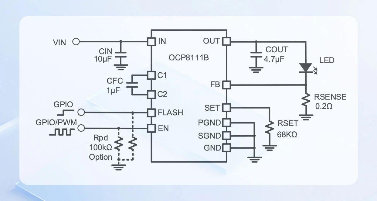
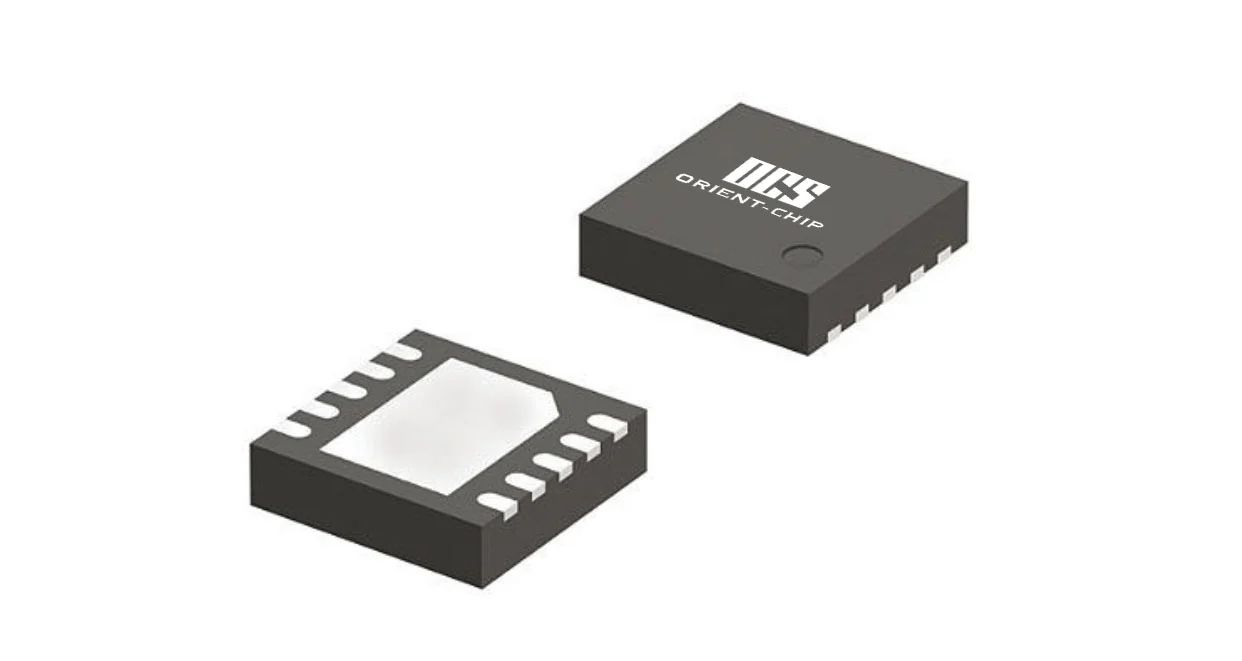
The OCP8111B integrates internal pull-down resistors on the EN and FLASH pins, eliminating the need for external pull-down resistors and thereby reducing system costs. The device features a higher output current capability of 1.2 A and incorporates comprehensive protection mechanisms—including LED short-circuit, output short-circuit, input under-voltage, output open-circuit, and over-temperature protection—ensuring safe and reliable operation. It is available in a 3 mm × 3 mm DFN-10L package, which is green, lead-free, and halogen-free.
Principles and Advantages of PWM Dimming
As illustrated in the figure below, the PWM signal is applied to the EN pin; via a push-pull circuit, the amplitude of the PWM signal is converted into VREF while preserving the duty cycle information. The RC low-pass filter circuit then removes the AC components of the converted PWM signal, yielding the DC component, which is then applied to the EA pin as the internal feedback (FB) reference voltage, thereby establishing a steady-state LED current.
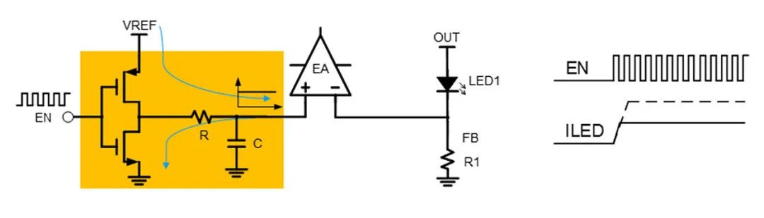
LED formula for calculating the current is as follows:
ILED = VREF * D / R1 ,
From this, it can be observed that the LED current exhibits a linear relationship with the duty cycle D.
The measured waveform is as follows:
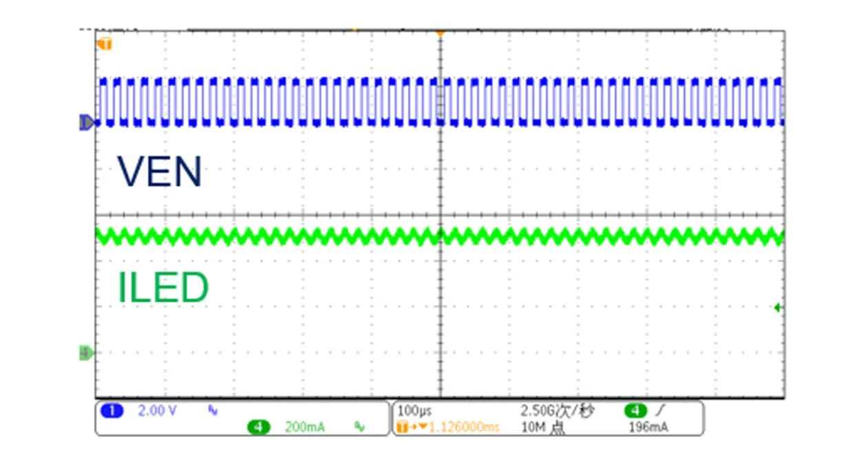
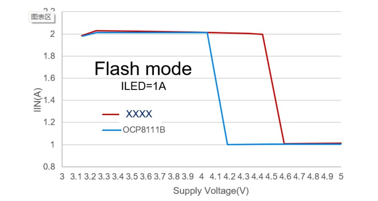
The PWM dimming mode of the OCP8111B not only achieves extremely low current ripple but also offers significant advantages in power consumption. As shown in the figure below, under identical lamp voltage and current conditions, the OCP8111B only enters the 2x mode when VIN drops to 4.2 V, resulting in power consumption that is substantially lower than that of comparable products.