OCP2137 – a high-efficiency power management chip specifically tailored for AMOLED displays


Background of the AMOLED
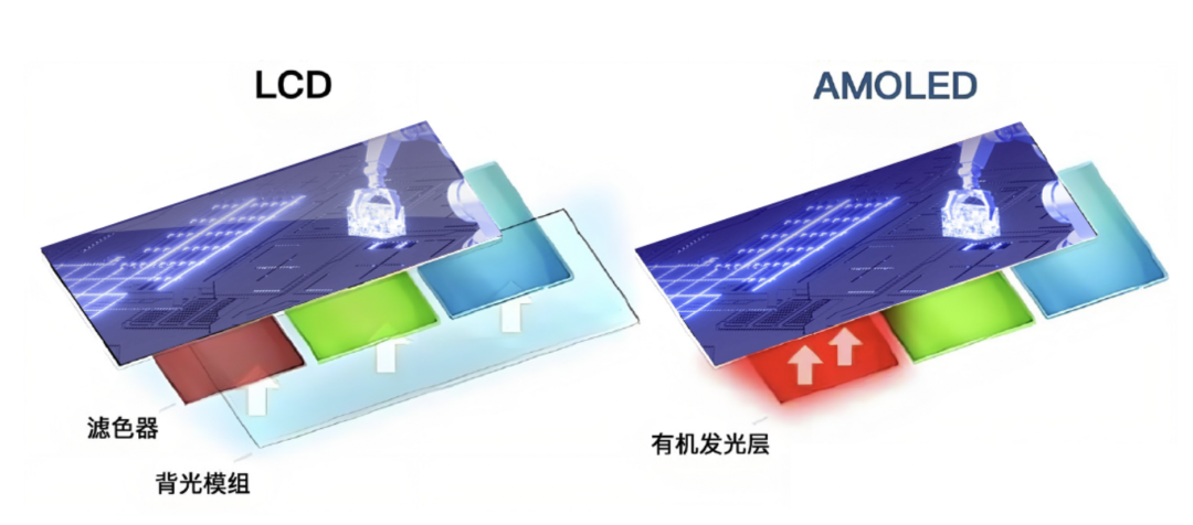
With the rapid development of smart electronic devices, display screen technology has also been advancing continuously. AMOLED (Active Matrix Organic LED) displays—characterized by their slim profile, fast response times, self-e missive capability, flexible design, and wider color gamut—have gradually supplanted LCDs as the market mainstream, becoming the preferred choice for high-end display applications.
OCP2137 Product Introduction
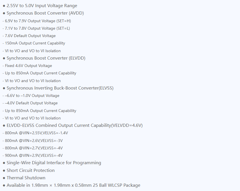
OCP2137 is a power management chip specifically designed for mobile phone AMOLED displays. It features three output voltage rails (AVDD, ELVDD, and ELVSS), supports one-wire communication and programmable output voltages, and delivers an output current of up to 850 mA, enabling it to meet the complex power requirements of AMOLED displays.
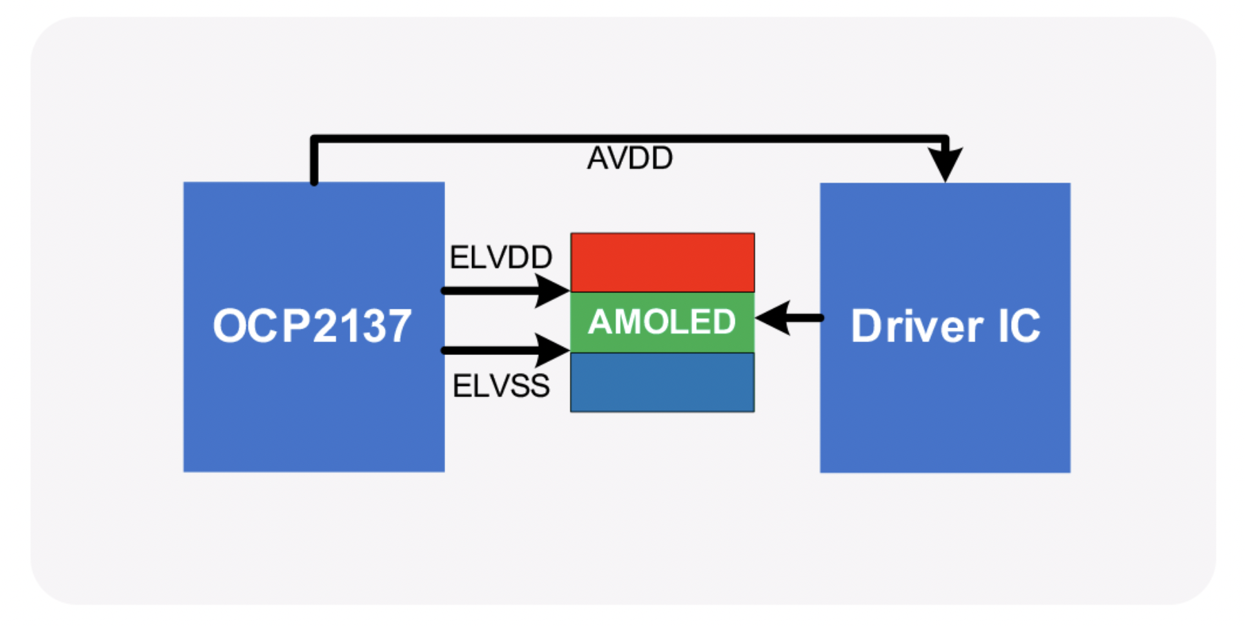
OCP2137 is a highly integrated AMOLED power solution that combines a boost converter (ELVDD), a negative voltage buck converter (ELVSS), and a boost converter (AVDD), making it suitable for battery-powered devices. The AVDD switch is controlled via the ASWIRE pin, the ELVDD and ELVSS switches are controlled via the ESWIRE pin, and the output voltages of VO2 and VO3 can be programmed via the SWIRE pin.
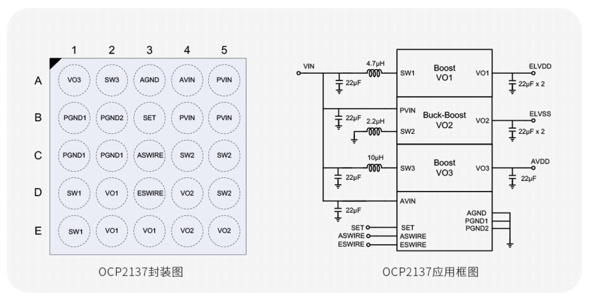
The OCP2137 features the WLCSP-25B package, providing an optimized PCB layout solution.
Technical breakthrough
Water ripple flicker effect
During the AMOLED display process, as shown in the figure below, ELVDD is applied to the source terminal of the drive PMOS, while ELVSS is applied to the cathode of the OLED.
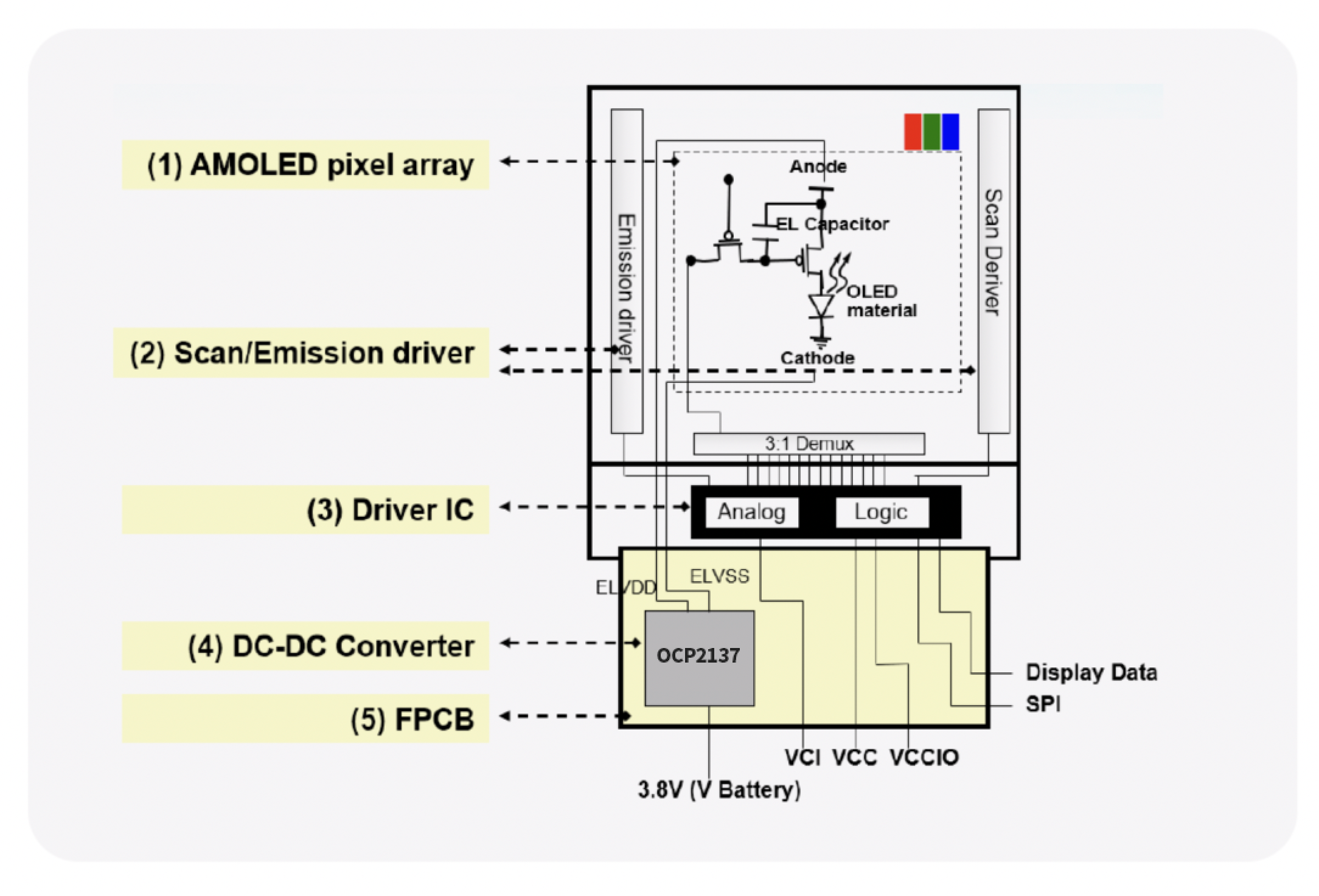
Current equation for the luminescent stage:

Vs=ELVDD. Consequently, voltage jitter in ELVDD can induce current variations, which, to the human eye, manifest as image jitter—namely, screen flicker and water ripple effects.
Current during the fully black phase:
At this stage, turning off the PMOS driver ensures sufficient discharge of the OLED, and the voltage across the OLED affects the current variation; since ELVSS is applied to the cathode of the OLED, voltage jitter in ELVSS can also impact image display.
Circuit-level optimization for water ripple and flicker phenomena:
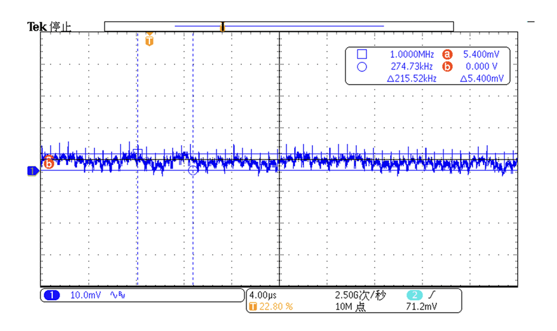
Since the ELVDD is derived from a BOOST switching circuit, switching ripple—particularly low-frequency ripple under light load—may occur. To address this issue, a forced-continuous BOOST topology is introduced to ensure that the ELVDD ripple remains at a high frequency (above 1.3 MHz), which is imperceptible to the naked eye, with its amplitude controlled at approximately 5 mV.
Although the impact of ELVSS is relatively small, it still exists; therefore, ripple optimization has also been applied to the ELVSS ripple amplitude: in the ELVSS light-load mode, an intentional interference is introduced in the switch-on detection circuit; under the light-load low-frequency mode, the switching frequencies and number of switches are relatively uneven and dispersed, thereby reducing the risk of flicker at low brightness levels; the ripple amplitude is kept within 10 mV.
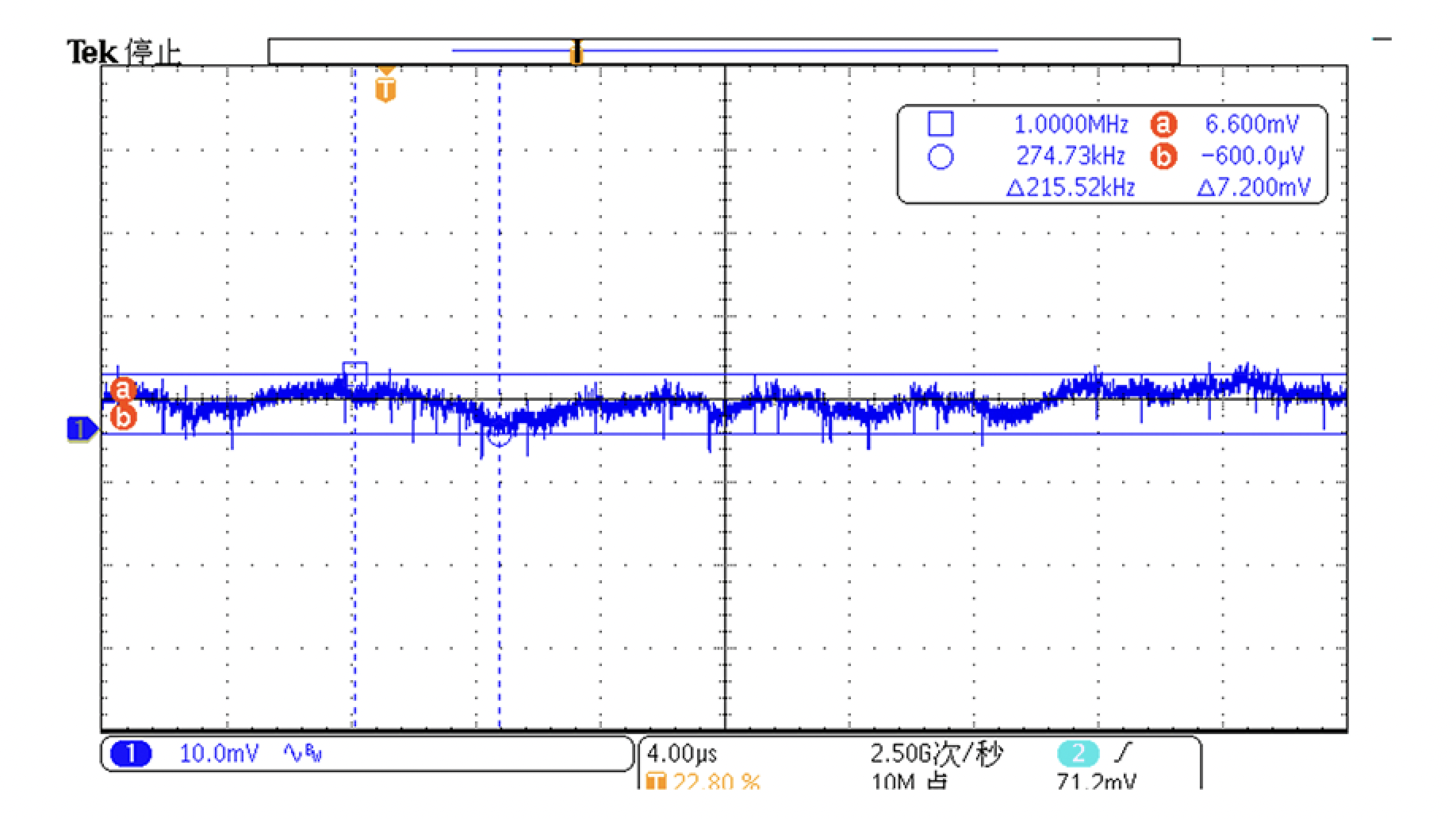
The comprehensive reduction of output voltage ripple ensures an exceptional visual experience across a wide range of display scenarios.
Increase in supply voltage
Currently, some mobile phones are used during charging, during which the supply voltage may exceed 4.6V due to voltage fluctuations. Since the output voltage of ELVDD is also 4.6V, the ELVDD BOOST topology cannot achieve a 100% duty cycle, leading to abnormal output voltage. To address this issue, the following measures are implemented: introducing DIODE MODE; utilizing the parasitic diode of the power transistor to perform voltage reduction, whereby when the input voltage approaches the output voltage, the parasitic diode dissipates a portion of the voltage; consequently, the OCP2137 can support an input voltage of up to 5V.
Improvement in current capability under the trend toward high brightness in AMOLED displays
Have you ever experienced this when using your phone outdoors: on a scorching summer day, under the bright sunlight, you find that the images on your phone become blurry? To address this issue, high-brightness technology has now been integrated into mobile phone development: when ambient light levels are high, the screen enters high-brightness mode; this, in turn, places greater demands on our power management chips (requiring higher current capacity).
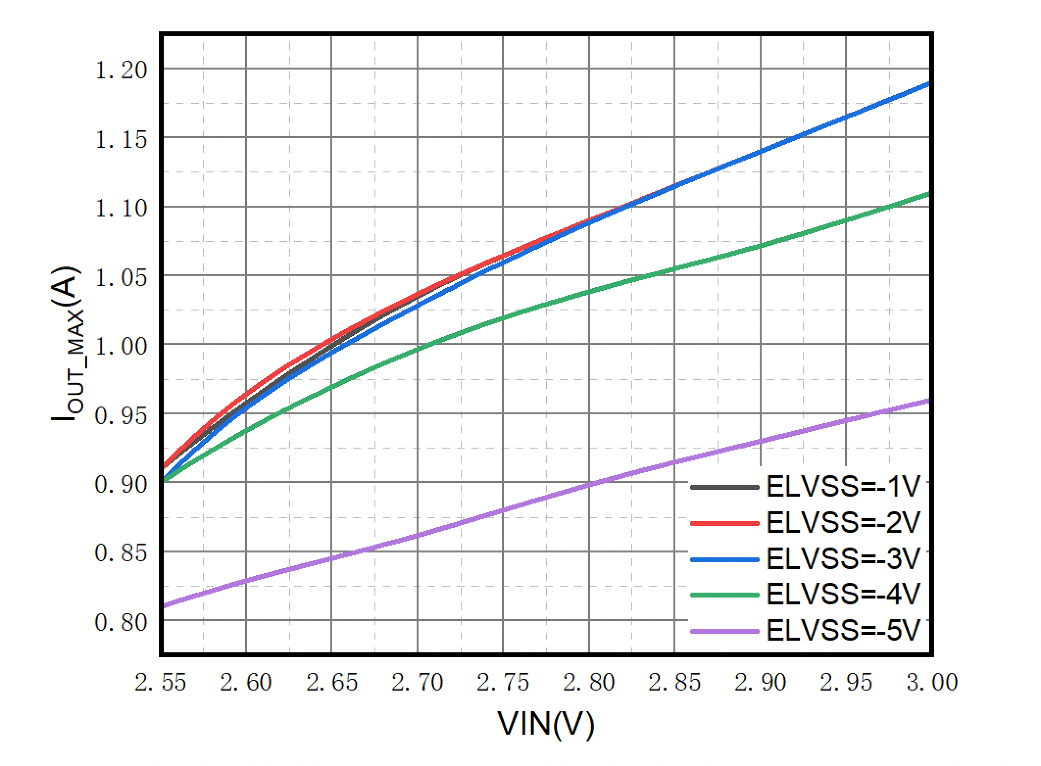
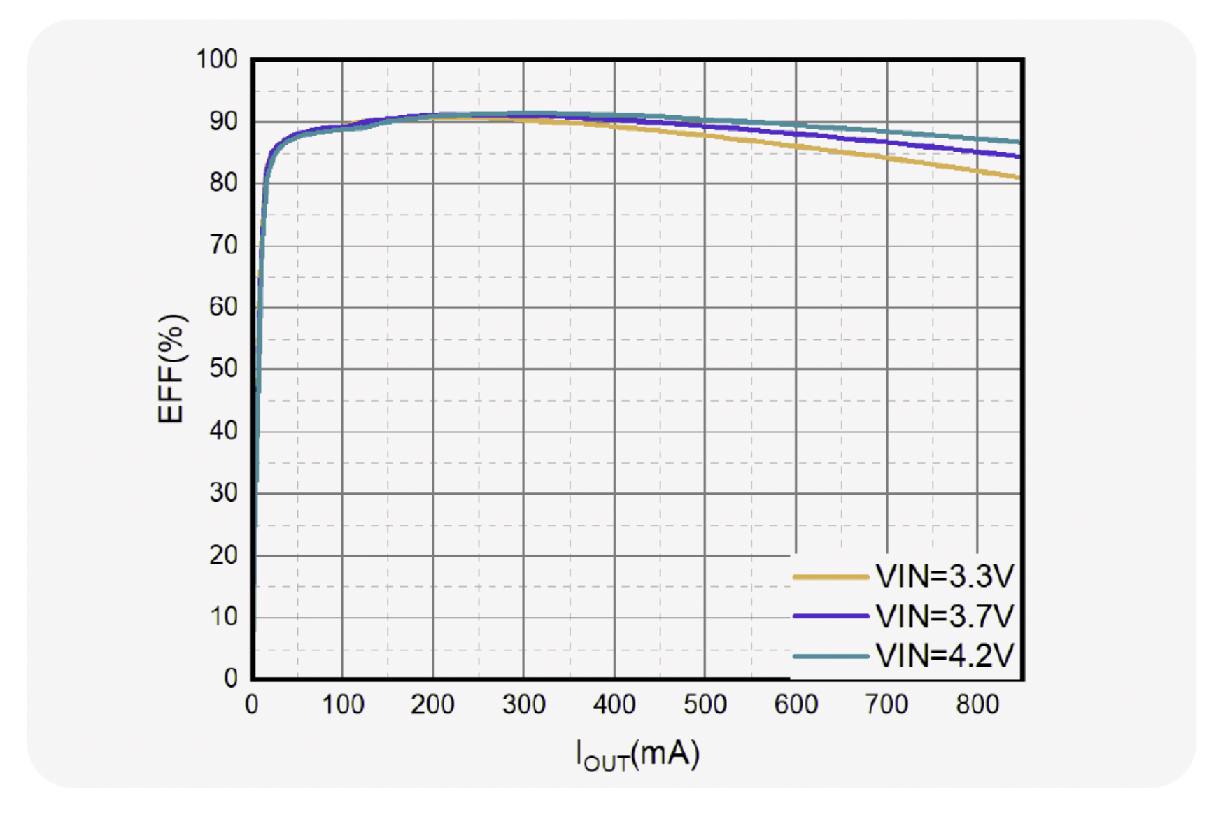
In terms of current capability, OCP2137 maintains a load current of over 800 mA even under conditions of low input voltage and high output voltage, making it suitable for displays requiring brightness levels above 1500 nits.
Efficiency improvements amid the trend toward low power consumption
With the continuous advancement of power management chips, as output capabilities increase, there are also stringent requirements for power consumption in order to extend the overall battery life of mobile phones. Big data analysis indicates that the optimal operating environment for users is within 200 nits to 400 nits, corresponding to an output current range of 100 mA to 300 mA; in high-brightness mode, however, currents exceeding 800 mA are typically required. The OCP2137 chip has been specifically optimized for the 100 mA–300 mA range, achieving peak efficiency of up to 92%, while also maintaining over 80% efficiency even at maximum current loads.
Product Features of OCP2137
1. An output voltage ripple below 1.10 mV ensures an exceptional visual experience;
2. Supports a battery voltage range of 2.55 V–5 V, while guaranteeing a current capacity of over 800 mA at an output voltage of ELVDD = 4.6 V and ELVSS = –5 V; 3. Achieves up to 92% efficiency to improve mobile phone battery life.