OCA72559FQAD
10.5V, High PSRR, Low Noise Mono Class D Amplifier with AGC
- Vin2.7V~5.5V
- PVDD10.5V
- Pout@Rload=8Ω & THD+N=1%5.4W@ VIN=4.2V
- Boost TypeAdaptive Boost
- Receiver ModeYes
- ProtectionMulti-Level AGC with Zero-ADJ
-
Overview
-
Features
-
Specifications
-
Package & Ordering
-
Apply
overview
OCA72559FQAD is a mono, filter-free Class D audio power amplifier with optimized automatic gain control (AGC) and synchronous Boost. AGC functions are not only configured to prevent audio signal distortion but also to enhance sound quality and volume automatically. It also can be configured to protect the speaker from damage at high power levels. The high voltage boost achieves high output voltage which can improve music signal dynamic range significantly. OCA72559FQAD is cable of driving 6.1W at 4.2V into a 6Ω load or 5.4W at 4.2V into a 8Ω load with speaker mode.
OCA72559FQAD also supports speaker and receiver 2-in-1 application. In receiver mode, the noise floor can be achieved 9uVrms and total harmonic distortion (THD) can be achieved 0.008% with 0.1W at 4.2V into a 8Ω load.
In addition to these features, I2C interface makes easier commutation between AP and OCA72559FQAD.
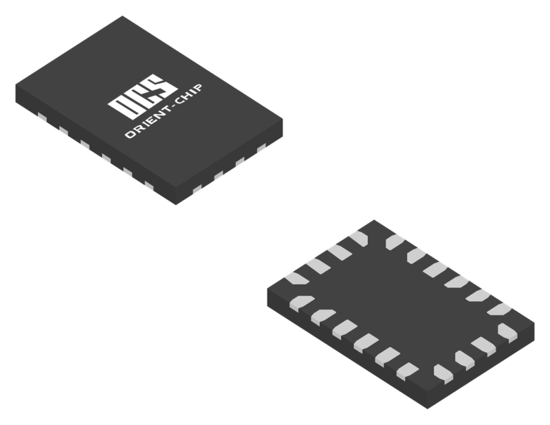
The device is a RoHs compliant FCQAD 2mm x 3mm x 0.55mm -20L package.
Applications
Smartphones, Cellphone, PDAsBluetooth, wireless handsetsPortable equipment
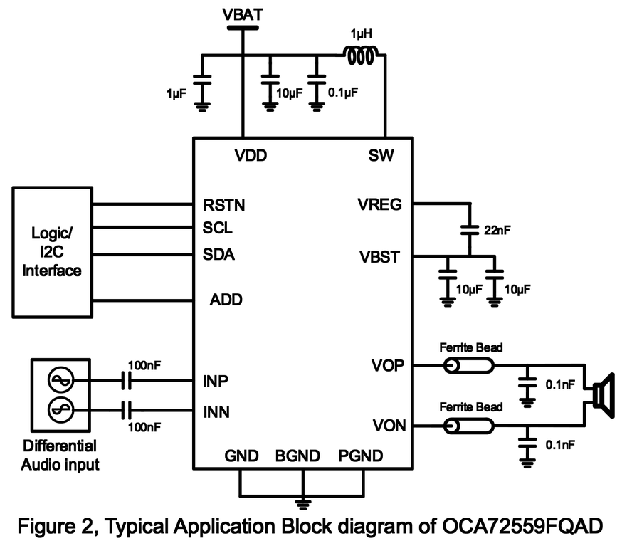
Typical Application Circuit
features
-
 Power Voltage Range: 2.7V to 5.5V
-
Boost Output Voltage Ranger: up to 10.5V
-
Support Speaker & Receiver 2-in-1 mode
-
Overall Efficiency up to 85
-
Output power 5.4W@8Ω, 6.1W@6Ω
-
Adjustable speaker-guard power level: 0.5W~2W@8Ω, 100mW/Step
-
Low Noise: 9uVrms (Class D Receiver@0dB), 18uVrms (Class D Receiver@9dB), 35uVrms (Class D Speaker@18dB)
-
PSRR: -82dB @ 217Hz
-
Optimized AGC control for sound quality
-
Battery tracking for low voltage protection
-
Excellent TDD noise suppression and POP-Click noise suppression
-
Shut Down Current: 0.1μA
-
Support 1.8V I2C interface
-
FCQFN20L, 2mm x 3mm x 0.55mm
Specifications
-
Vin2.7V~5.5V
-
PVDD10.5V
-
Pout@Rload=8Ω & THD+N=1%5.4W@ VIN=4.2V
-
Boost TypeAdaptive Boost
-
Receiver ModeYes
-
ProtectionMulti-Level AGC with Zero-ADJ
-
Control InterfaceI2C
-
PackageFCQFN-20L
Package & Ordering
Package & Pin Definition
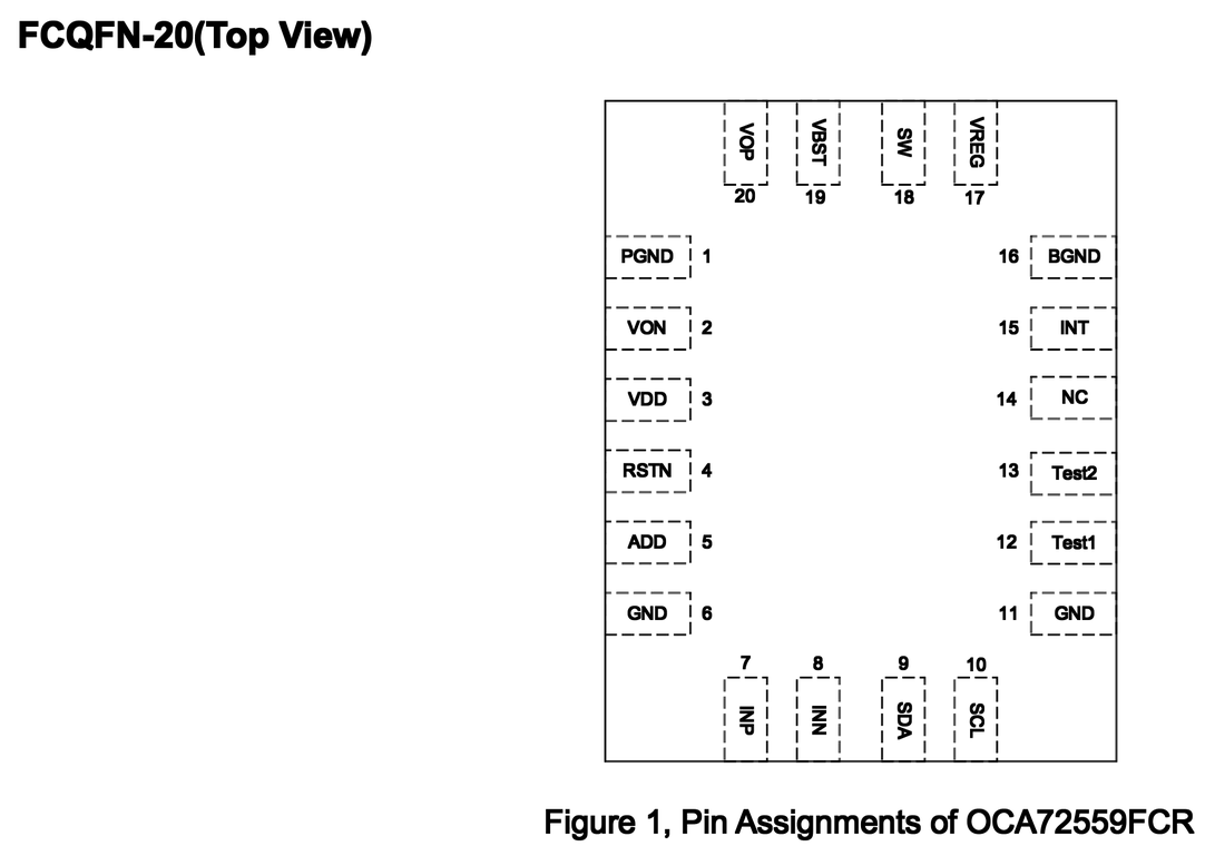
| Pin Name | Pin No. FCQFN-20L | Pin Function |
|---|---|---|
| PGND | 1 | Class D power ground |
| VON | 2 | Negative audio output terminal |
| VDD | 3 | Power supply |
| RSTN | 4 | Reset pin, active low reset, the internal 2MΩ pull-down resistor in chip |
| ADD | 5 | I2C slave address pin |
| GND | 6 | Ground |
| INP | 7 | Positive audio input terminal |
| INN | 8 | Negative audio input terminal |
| SDA | 9 | I2C data |
| SCL | 10 | I2C clock |
| GND | 11 | Ground |
| TEST1 | 12 | TEST pins, connect to GND in application |
| TEST2 | 13 | TEST pins, connect to GND in application |
| NC | 14 | NC pins, connect to GND in application |
| INT | 15 | INT pins, connect to GND in application |
| BGND | 16 | Boost power ground |
| VREG | 17 | Charge pump output pin |
| SW | 18 | Boost switch pin |
| VBST | 19 | Boost output pin |
| VOP | 20 | Positive audio output terminal |