


OCP8223
QR PWM Controller IC for Wide-Voltage-Output Current Mode
- Series DescriptionIsolated SSR Controller
- FeaturesExternal D-GaN Drive
- Power transistor100W
- Output Power9-70V
-
Overview
-
Features
-
Specifications
-
Package & Ordering
overview
The OCP8223W is a highly integrated quasi-resonant (QR) current-mode PWM controller. Its ultra-wide VCC operating voltage range meets the requirements of PD fast-charging power supplies.
The OCP8223W uses green energy-saving mode, burst mode, and QR and PFM modes at medium and heavy load to optimize system efficiency, significantly improving it.
The OCP8223W integrates proprietary patented soft start, frequency jittering and slope compensation, greatly improving system stability, reliability and electromagnetic compatibility. Its patented VCC operating voltage range is 9V-70V. It is a high-performance, low-EMI, low-standby-power solution for PD fast-charging power supplies with a wide output voltage range.
The OCP8223W provides a complete set of proprietary patented protection functions, including input under-voltage protection (BNO), VCC under-voltage protection, VCC over-voltage protection, output over-voltage protection, output under-voltage protection, short-circuit protection, external over-temperature protection, internal over-temperature protection, GATE clamp protection, CS pin short-circuit protection, CS soft start, secondary rectifier short-circuit protection, and comprehensive system-level protection with automatic restart upon abnormal conditions.
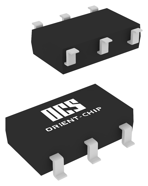
The OCP8223W is available in an SOT23-6L package.
Applications
PD/QC fast chargersAdaptersSwitching power supplies
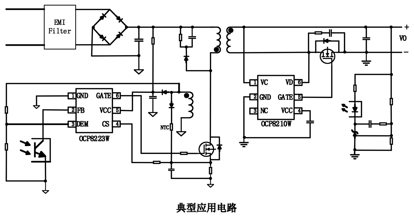
Typical Application Circuit
features
-
 Ultra-wide VCC operating voltage 9V-70V
-
Meets Level 6 energy efficiency standard
-
Input under-voltage protection
-
Adaptive QR/PFM/burst multi-mode regulation
-
Secondary-side constant power output
-
External/internal over-temperature protection (OTP)
-
Line voltage BNO
-
Hysteretic VCC under-voltage lockout and VCC over-voltage protection
-
Output over-voltage protection (OVP)
-
Output short-circuit protection (SCP)
-
Output diode short-circuit protection
-
CS/FB pin short-circuit protection
-
Can drive external D-GaN power devices
Specifications
-
Series DescriptionIsolated SSR Controller
-
FeaturesExternal D-GaN Drive
-
Power transistor100W
-
Output Power9-70V
Package & Ordering
Package & Pin Definition
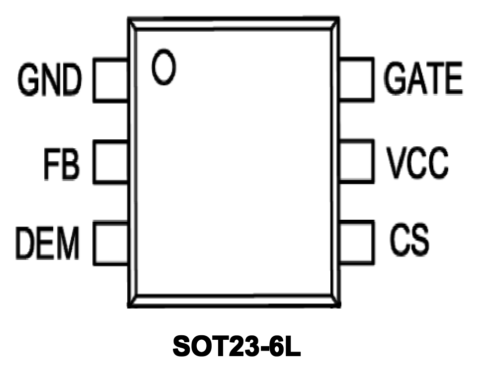
| Pin No. | Name | I/O | Description |
|---|---|---|---|
| 1 | GND | P | Reference ground |
| 2 | FB | I | Feedback input pin; the voltage on this pin and the CS pin signal determine the PWM duty cycle |
| 3 | CS | I | Multi-function pin, enabling BNO, OVP, UVP, demagnetization detection, etc. |
| 4 | DEM | I | Current sense signal; with an external diode and NTC, enables OTP, OCP, etc. |
| 6 | VCC | P | Chip power supply |
| 6 | GATE | I | Gate drive for the power MOSFET |