OPS1121A
Qi 1.2.4 Compliant High-Efficiency Wireless Charging Receiver
- WPC ProtocolQI BPP 5W
- EEPROM Size256 Bytes
- Operation ModeLDO
- Maximum Output Voltage5V
- Maximum Output Current0.7A
- Input Voltage≤20V
-
Overview
-
Features
-
Specifications
-
Package & Ordering
-
Apply
overview
The OPS1121A is a highly integrated, high-efficiency, low-power wireless charging receiver chip designed for Qi BPP. It integrates a wireless receiving full-bridge rectifier, a linear regulator, the Qi wireless charging protocol and a wired-charging switch path. The OPS1121A requires only a few external components and no firmware programming, delivering stable and reliable performance for a minimalist low-power wireless charging receiver solution.
The OPS1121A has a typical output voltage of 5.0V and a maximum output current of 800mA. The chip supports dynamic adjustment of the Vrect output for the best dynamic switching response and heavy-load efficiency. Charging efficiency under heavy load exceeds 80%①, and it supports external NTC temperature regulation and various protection functions including UVLO, OVP and OTP. The on-chip EEPROM allows adjustment of all key charging parameters, adapting to various small coils with strong Qi certification compatibility.
The OPS1121A integrates a wired switch path, which can automatically detect power insertion and switch between wired and wireless charging. The chip integrates highly reliable wired over-voltage and over-current protection.
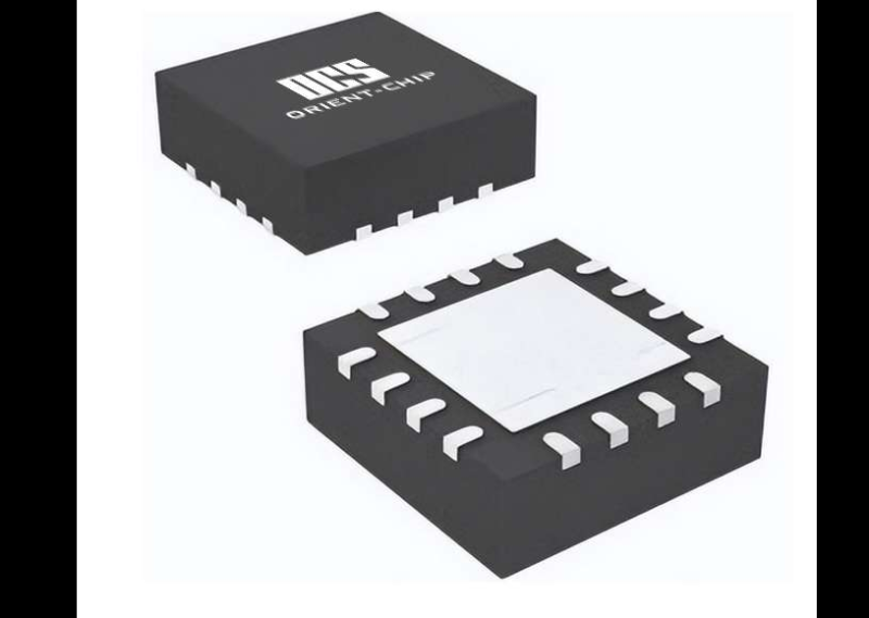
The OPS1121A is available in a 3mm x 3mm QFN-16pin package, supports I2C configuration, and enables a single-LED indication mode.
①: Measured with an 8.3uH small coil and an OPS1033 transmitter. Efficiency evaluation method: OPS1121A output power / transmitter input power, i.e., the efficiency of the whole system.
Applications
Personal care productsTWS charging cases and other portable charging casesConsumer wearable devicesSmart watchesWireless keyboards and mice
features
-
 Compliant with WPC Qi 1.2.4 standard, maximum output power 4W
-
Integrated wireless charging receiver protocol, ASK communication, synchronous rectification, LDO
-
LDO typical output voltage 5.0V, maximum output current 800mA
-
Dynamic rectifier output voltage for fast load response and high heavy-load efficiency
-
High-reliability architecture with rectifier output over-voltage clamp protection; supports input over-voltage, output over-current, internal and external over-temperature protection, programmable temperature control, indication and error detection.
-
Supports programming of key parameters for flexible configuration of protocol and chip parameters
-
Minimal external components, only 13 resistors and capacitors required
-
Supports automatic switching between wired and wireless modes, with all power MOSFETs integrated
-
Supports I2C interface for firmware upgrade, debugging and control
-
Supports single-LED indication
-
3mm x 3mm 0.5pitch QFN 16pin package
Specifications
-
WPC ProtocolQI BPP 5W
-
EEPROM Size256 Bytes
-
Operation ModeLDO
-
Maximum Output Voltage5V
-
Maximum Output Current0.7A
-
Input Voltage≤20V
-
OVP/OCP/OTPYes
-
PackagingQFN3X3-16
Package & Ordering
Ordering Information
| Part Number | Marking | Package Type | Package Qty | Temperature | Eco Plan | Lead |
|---|---|---|---|---|---|---|
| OPS1121A | CCX1121A | QFN3030-16L | 3000pcs | -40~85°C | Green | Sn |