


OPS1034A
Fully Integrated Wireless Charging Transmitter SoC with Boost and High-Frequency Drive
- WPC ProtocolQI2.0
- USB ProtocolQC3.0
- Input Voltage4 - 6.5V
- Output Power≤15W
- ASK decoderVoltage/Current/Phase
- Number of Charging LoadsSingle

-
Overview
-
Features
-
Specifications
-
Package & Ordering
-
Apply
overview
The OPS1034A is a wireless charging transmitter chip that supports boost and MHz high-frequency drive. It integrates, in a single chip, a boost controller, a full bridge with drivers, a high-performance 32-bit MCU, three-way (voltage/current/phase) adaptive demodulation, low-power high-precision Q-factor detection, a high-precision PWM and other core wireless charging modules. The OPS1034A can provide a smart-wearable transmitter solution with a minimal peripheral design, low temperature rise and high performance.
The OPS1034A has a built-in MCU with a maximum operating frequency of 24MHz, providing 32KB Flash and 4KB SRAM. It supports a 12-bit ADC with 3 external channel inputs, one 16-bit advanced controller and 4 general-purpose 16-bit timers, and provides up to 14 GPIOs.
The OPS1034A provides a dedicated high-precision PWM controller of up to 144MHz, supporting carrier drive output above 2MHz and adaptive dead-time control. The chip offers 15mV boost control accuracy, less than 15uA quiescent standby current, a built-in full-bridge MOS and a customizable Dither function, delivering excellent cost-effectiveness for smart-wearable solutions.
The OPS1034A provides fast hardware and software OCP, OVP, UVP and OTP protection solutions, ensuring stable operation of the chip over -20℃~85℃.
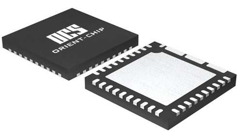
The chip is available in a 5x5mm QFN 34pin package.
Applications
Wireless fast charging for watchesWireless fast charging for smart hardware
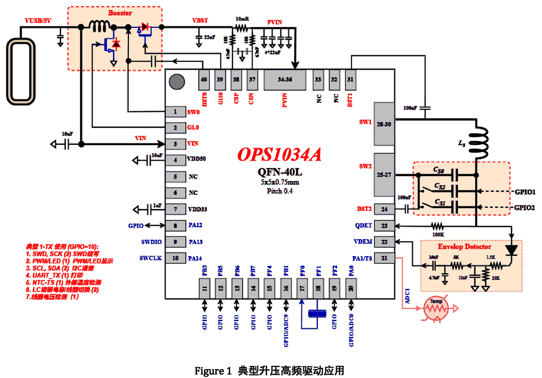
Typical Application Circuit
features
-
 VIN input voltage: 4V to 6.5V
-
Full-bridge input voltage: 4V to 16V
-
Integrated ultra-low on-resistance wireless charging full-bridge MOSFET (Rdson 17mΩ)
-
Integrated three-way (voltage/current/phase) adaptive demodulation
-
Integrated high-precision PWM generator of up to 144MHz
-
Integrated boost controller with 15mV control voltage accuracy
-
Standby current less than 15uA
-
Supports low-voltage high-precision Q-factor detection
-
Supports FSK modulation and Dither function
-
24MHz 32-bit MCU
-
32KB Flash, 4KB SRAM, 14 GPIOs
-
Supports fast OCP/OVP/OTP protection
Specifications
-
WPC ProtocolQI2.0
-
USB ProtocolQC3.0
-
Input Voltage4 - 6.5V
-
Output Power≤15W
-
ASK decoderVoltage/Current/Phase
-
Number of Charging LoadsSingle
-
MOS IntegratedYes
-
Flash Size32KB
-
Boost Controller IntegratedYes
-
PackagingQFN 5x5 34pin
Package & Ordering
Ordering Information
| Part Number | Marking | Package Type | Package Qty | Temperature | Eco Plan | Lead |
|---|---|---|---|---|---|---|
| OPS1034A | OPS1034A | QFN5050-40L | 3000pcs | -40~85℃ | Green | Sn |

