OCP1310
1A, Low IQ, High PSRR CMOS LDO
- Vin1.8V~5.5V
- Output Range1.8V/2.5V/2.8V/3.0/3.3V
- Output Current1000mA
- PSRR58dB @217Hz 60dB @1KHz
- Noise40μVrms
- Dropout120mV@1A
-
Overview
-
Features
-
Specifications
-
Package & Ordering
-
Apply
overview
OCP1310 is a low dropout, low power linear regulator which operates from 1.8V to 5.5V input voltage. OCP1310 provides high power supply rejection ratio (PSRR) and delivers up to 1A output current. OCP1310 also offers low current consumption for battery operated applications.
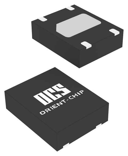
The device is available in a RoHS compliant DFN1612-8L package.
Applications
Smart phones, Cell phone, PDAsBluetooth, wireless handsetsPortable equipment
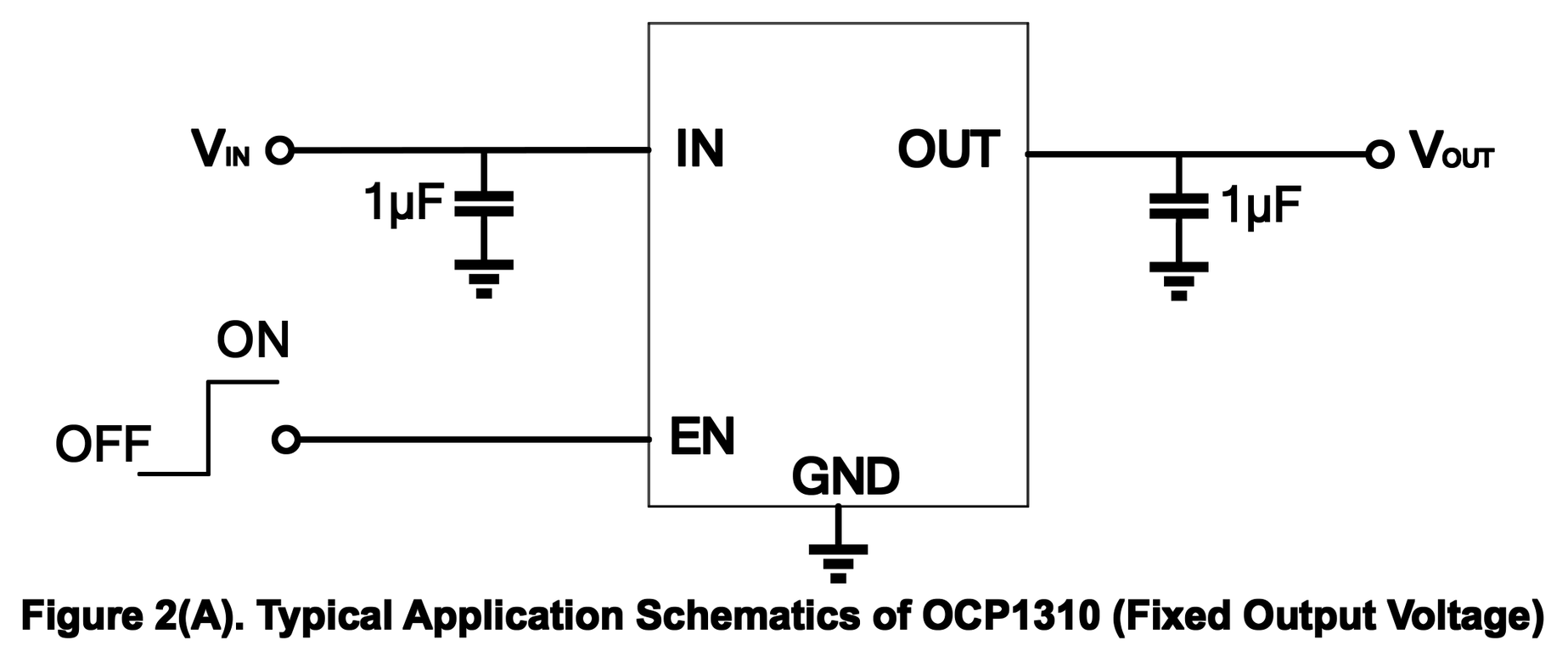
Typical Application Circuit
features
-
 Input Voltage Range: 1.8V to 5.5V
-
Fixed Output Voltage: 1.2V, 1.8V, 2.5V, 2.8V, 3.0V, 3.3V
-
Adjustable Output from 0.8V to 4.2V
-
Output Current Capability: 1A
-
Low Quiescent Current: 70μA (Typ)
-
Shutdown Current: 0.01μA (Typ)
-
Power Supply Rejection Ratio: typical 70dB (IOUT=30mA, Freq=1kHz)
-
Typical 120mV dropout voltage at 1A load, VOUT=3.3V
-
Noise: typical 40uVrms (IOUT=30mA, BW=10Hz to 100kHz)
-
Built-in Output Short Protection: typical 250mA when output short to ground
-
Auto-Discharge Function
-
Available in DFN1612-8L Package
Specifications
Type
Parameter
Type
Parameter
-
Vin1.8V~5.5V
-
Output Range1.8V/2.5V/2.8V/3.0/3.3V
-
Output Current1000mA
-
PSRR58dB @217Hz 60dB @1KHz
-
Noise40μVrms
-
Dropout120mV@1A
-
PackageDFN1216
Package & Ordering
Ordering Information
| Part Number | VOUT(V) | Marking | Package Type | Package Qty | Temperature | Eco Plan | Lead |
|---|---|---|---|---|---|---|---|
| OCP1310V12AD | 1.2 | DT | DFN1612-8L | 3000pcs | -40~85°C | Green | Sn |
| OCP1310V18AD | 1.8 | ET | DFN1612-8L | 3000pcs | -40~85°C | Green | Sn |
| OCP1310V25AD | 2.5 | FT | DFN1612-8L | 3000pcs | -40~85°C | Green | Sn |
| OCP1310V28AD | 2.8 | KT | DFN1612-8L | 3000pcs | -40~85°C | Green | Sn |
| OCP1310V30AD | 3.0 | MT | DFN1612-8L | 3000pcs | -40~85°C | Green | Sn |
| OCP1310V33AD | 3.3 | AT | DFN1612-8L | 3000pcs | -40~85°C | Green | Sn |
| OCP1310V00AD | ADJ | NT | DFN1612-8L | 3000pcs | -40~85°C | Green | Sn |
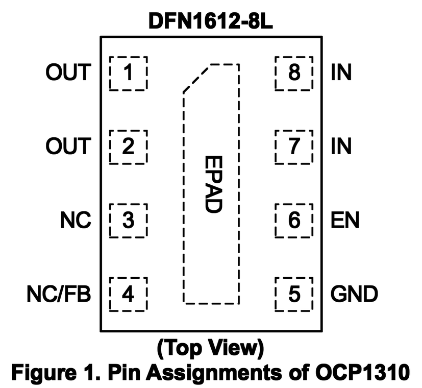
Package & Pin Definition
| Pin Name | Pin Number | Pin Function |
|---|---|---|
| OUT | 1, 2 | Regulator Output Pin. |
| NC | 3 | No Connection. |
| NC/FB | 4 | NC for fixed output voltage version, no connection. FB for adjustable output voltage version, output voltage feedback pin. Connect to output voltage with feedback resistor divider. |
| GND | 5 | Ground pin. |
| EN | 6 | Chip enable input pin, active high. |
| IN | 7, 8 | Power supply input pin. |
| EPAD | EPAD | Thermal Pad. It's recommended to connect the EPAD to GND plane. |