OCP14051
500mA, Low Dropout, Low Noise, High PSRR CMOS LDO
- VinVout+Do~5.5V
- Output Range1.0V/1.05/1.1V/1.2V/1.8V/3.3V
- Output Current500mA
- PSRR85dB @217KHz 76dB @1KHz
- Noise35μVrms
- Dropout150mV @0.5A
-
Overview
-
Features
-
Specifications
-
Package & Ordering
-
Apply
overview
OCP14051 is a 500mA low dropout, low power linear regulator with NMOS pass transistor and a separate bias supply voltage. OCP14051 provides stable and accurate output for noise sensitive applications. OCP14051 also offers low current consumption for battery operated applications.
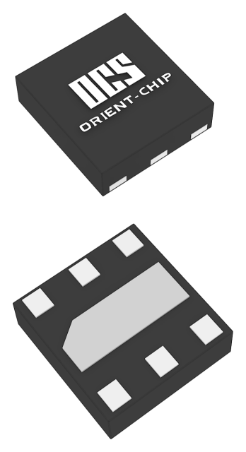
The device is a RoHS compliant DFN1212-4L package.
Applications
Smartphones, Cellphone, PDAsBluetooth, wireless handsetsPortable equipment
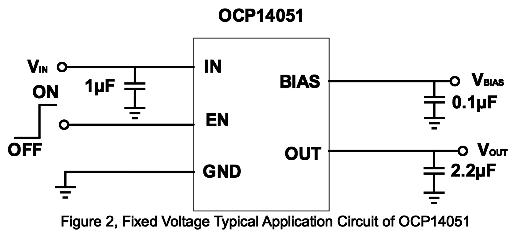
Typical Application Circuit
features
-
 Input Voltage Range: 0.8V to 5.5V
-
Bias Voltage Range: 2.6V to 5.5V
-
Output Voltage Ranger: 0.8V to 3.6V
-
Output Current: 500mA
-
Low Quiescent Current: 70μA(Typ)
-
Shut Down Current: <1μA
-
Dropout Voltage: 150mV @ 500mA
-
PSRR-VIN: 70dB @ 1kHz
-
PSRR-VBIAS:78dB @ 1KHz
-
Auto-Discharge function
-
Available in DFN1212-4L package
-
-40°C to +85°C Operating Temperature Range
Specifications
Type
Parameter
Type
Parameter
-
VinVout+Do~5.5V
-
Output Range1.0V/1.05/1.1V/1.2V/1.8V/3.3V
-
Output Current500mA
-
PSRR85dB @217KHz 76dB @1KHz
-
Noise35μVrms
-
Dropout150mV @0.5A
-
PackageDFN1.2*1.2-4L
Package & Ordering
Ordering Information
| Part Number | VOUT(V) | Marking | Package Type | Package Qty | Temperature | Eco Plan | Lead |
|---|---|---|---|---|---|---|---|
| OCP14051V09AD | 0.9 | CW | DFN1212-4L | 3000pcs | -40~85℃ | Green and RoHS | Sn |
| OCP14051V10AD | 1.0 | CY | DFN1212-4L | 3000pcs | -40~85℃ | Green and RoHS | Sn |
| OCP14051V105AD | 1.05 | CU | DFN1212-4L | 3000pcs | -40~85℃ | Green and RoHS | Sn |
| OCP14051V11AD | 1.1 | CR | DFN1212-4L | 3000pcs | -40~85℃ | Green and RoHS | Sn |
| OCP14051V12AD | 1.2 | CS | DFN1212-4L | 3000pcs | -40~85℃ | Green and RoHS | Sn |
| OCP14051V125AD | 1.25 | CV | DFN1212-4L | 3000pcs | -40~85℃ | Green and RoHS | Sn |
| OCP14051V18AD | 1.8 | CT | DFN1212-4L | 3000pcs | -40~85℃ | Green and RoHS | Sn |
| OCP14051V33AD | 3.3 | CD | DFN1212-4L | 3000pcs | -40~85℃ | Green and RoHS | Sn |
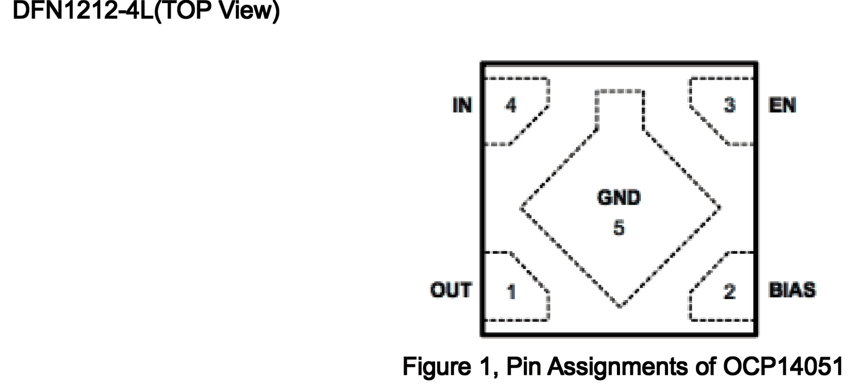
Package & Pin Definition
| Pin Name | Pin Number | Pin Function |
|---|---|---|
| OUT | 1 | Regulator Output Pin. It is recommended to use output capacitor with effective capacitance in the range 1μF to 10μF. |
| BIAS | 2 | Bias Voltage Supply for Internal Control Circuits. This pin is monitored by internal under-voltage lockout circuit. |
| EN | 3 | Enable Pin. Driving this pin high enables the regulator. Driving this pin low puts the regulator into shutdown mode. |
| IN | 4 | Input Voltage Supply Pin. |
| GND | 5 | Ground. |